As part of an effort to share more designs, I’ve decided to start writing a continuing series of blog articles on my hardware design efforts. This first article covers the NixieBoost of a NixieView.
Background
Despite being purely software focused at my current job, previous experience and work has been very hardware and firmware focused. I really do enjoy getting my hands dirty, designing, fabricating, prototyping, and debugging hardware. I don’t consider myself a “maker”, preferring to dive into the true technical foundations.
A “required” project in this day and age (for any hipster, and non-hipster) is a Nixie clock. Somehow I totally missed the boat on this whole past-time, and do not actually have a clock! Due to some eBay accidents, I am the owner of large number of “tubes” (mainly, the Phillips ZM1000). As Nixie tubes are effectively neon tubes (they are not vacuum tubes), they require a high voltage to excite the gas (approximately 170V).
While its easy to rectify 170VDC directly from 120VAC mains, this requires a bulkier low-frequency isolation transformer for safety, and has limited flexibility. If the intent is to power the tubes from a common low-voltage supply (12V or so), a voltage boost converter needs to be employed to raise the isolated 12V to the needed 170V.
There are a few topologies available for raising the voltage, including a standard boost converter, as well as flyback and forward converters. The ratio of 12:170 is on the high end, and common design here would dictate a transformer coupled forward converter, however the output current required is very low: about 10 mA at 170V. This means it is still possible to get away with the more readily available boost converter power supply topology.
The boost converter
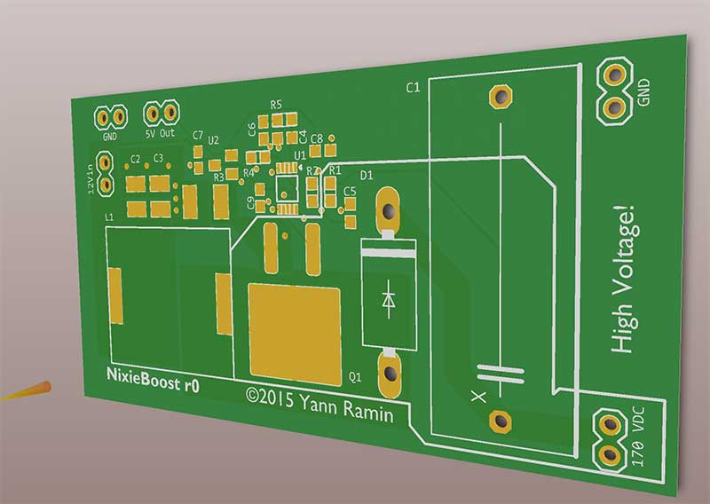
Building on the basic boost converter idea, I ended up with the revision 0 design as seen laid out above. The board is a mere 2.6 x 1.4inches. The following schematic is all the main juicy bits of the revision 0 design:

This design is built on the LTC1871 boost controller, a discrete high-current MOSFET (significantly over-specced, an Infineon IPB600N25N3), sense resistor, as well as any support circuitry and feedback network so the converter can sense the output voltage it is providing. Final output filtering is provided by a high voltage film capacitor. A secondary 5V LDO regulator is provided by an MCP1754, for later micro-controllers on the main board along with a power-supply for the RUN pin on the LTC1871.
Simulations

Any good analog circuit goes through a simulation validation phase. In this case, the above circuit was the first version drawn before the main board-level schematic, in order to validate component selection and general feasibility. The software used for simulation was LTspice.
The inductor is modeled using a saturation current, which is missing from the base model for inductors. Specifically:
flux={L*Is}*tanh(x/{Is}) ; L= inductance and Is= “saturation” current
As the conversion ratio is very large, somewhat large currents will be generated through the main switch node.
![DO5040H][inductor]
Inductor size was chosen for a low DCR, and a high saturation current. Primarily for low DCR (reducing resistive losses), an oversize 68uH inductor was chosen.
- 68mOhm DC resistance.
- 6.7A Isat
- 3.4A Irms
The simulation results show large switch currents, and high peak (0.7A) power, in the steady state:
![steady][simchart]
- V(n010) (blue) is the voltage at the switch node (after the inductor, and before the MOSFET)
- V(n006) (red) is the gate control to the FET from the LTC1871
- I(L) is the current through the inductor.
The switch speed chosen here is approximately 250kHz.
Whats next
Boards and components have been ordered from OSHPark / DigiKey - stay tuned for Part 2!
[simchart]: /images/nixieboost/sim_chart.png “Sim chart”" [inductor]: /images/nixieboost/do5040h.jpg